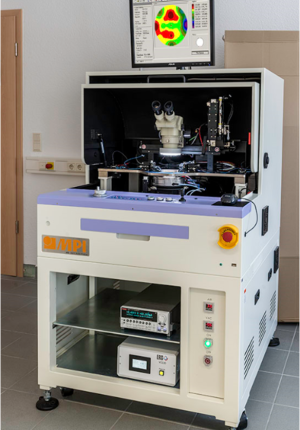
VI Systems new semi-automatic wafer prober station performs electrical and optical testing of wafers early in the manufacturing process. The system reduces manufacturing costs by eliminating out of specification wafers before they have been cut and packaged to improve yield. We offer 100% wafer characterization of 2” to 8” wafer structures. The test temperature ranges from 25°C to 150°C. Measurement of L-I-V parameters, threshold current, slope efficiency, optical spectrum, photo-diode sensitivity, reverse bias and dark current can be performed on each device.
Wafermap software analysis
Our software can import data files from various tools. The imported data can then be visualized or printed as line scans, contour plots, 2D plots or as a histogram. Several kinds of operations can be applied to the wafer maps such as rotation, shifting of the grid in the X or Y direction, or mirroring the data along the X or Y axis. Global operations such as adding or subtracting a constant or taking the 1st or 2nd derivative can be carried out. A sigma filter allows for the elimination of sites that exceed a user-defined range (e.g. measurement errors). It is also possible to compare different sets of data by adding, subtracting or dividing entire wafer map.

Wafer Mapping Software
See video of the mapping and software here:

 Vertically Integrated Systems
 Vertically Integrated Systems